Chapter 14
Bipolar Digital Circuits
As the final chapter of this text we shall investigate the two dominant bipolar digital circuit families in use today: transistor-transistor logic (TTL) and emitter-coupled logic (ECL). The chapter concludes with a brief investigation into the behavior of a simple digital circuit that combines both bipolar and MOS technology into a single technology referred to as BiCMOS.
14.1 Transistor-Transistor Logic (TTL)
The basic circuit for a TTL NAND gate is shown in part (a) of Fig. 14.1. It consists of four npn transistors Q1 - Q4, one diode D1, and several resistors. The input transistor Q1 consists of a single BJT with two emitters and is referred to as a multi-emitter transistor. This particular multi-emitter transistor can be viewed as two npn transistors connected in parallel as shown in Fig. 14.1(b). If Q1 has a single emitter then the NAND gate shown in Fig. 14.1(a) reduces to the basic TTL inverter circuit. With the aid of Spice, let us compute the voltage transfer characteristic of this gate from the A input to the NAND gate output. This is achieved by simply sweeping the dc voltage level at the A input between ground and the 5-volt supply. The B input will be connected to VCC=5 V throughout this simulation. In this arrangement, one emitter of the input transistor will be reverse biased, and the NAND gate will behave exactly like an inverter circuit. The fanout associated with this NAND gate will be set to one. It is necessary to load the output of the NAND gate so that realistic results can be obtained. The circuit arrangement used in this simulation is depicted in Fig. 14.1(c). The Spice deck for this situation is provided in Fig. 14.2. Notice that a subcircuit definition has been provided for the NAND gate. This is especially helpful when working with a large digital circuit consisting of many similar logic gates. Also, it is assumed that each resistor has a linear temperature coefficient of TC=+1200 ppm/°C. This will realistically model resistor behavior at different temperatures for the purpose of investigating circuit behavior versus temperature.
Running the Spice program on the above Spice deck results in the voltage transfer characteristic shown in Fig. 14.3. We see that the transfer characteristic consists of four main segments. With an input between 0 V and approximately 0.4 V, the output of the NAND gate is held constant at a level of 3.85 V. Beyond this input value of 0.4 V, but less than 1.2 V, the output voltage decreases at a linear rate of about -1.59 V/V. For inputs larger than 1.2 V, the output voltage deceases very quickly to a voltage level of about 0.111 V at an input voltage of 1.4 V. Above this value, the output voltage remains constant at 0.111 V. Based on this information, we can determine that VOL=0.111 V, VOH=3.85 V, VIL=0.423 V, and VIH=1.4 V. Thus, the low and high noise margins for this particular NAND gate with one input connected to VCC are 0.312 V and 2.45 V, respectively.
|
Fig. 14.1: (a) A two-input TTL NAND gate. (b) A multi-emitter bipolar transistor and its equivalent representation for Spice simulation. (c) A cascade of two NAND gates.
|
Voltage Characteristics Of A Two-Input TTL NAND Gate (Vb=logic 1)
* TTL Two-input NAND Gate .subckt NAND 10 9 4 1 * connections: | | | | * inputA | | | * inputB | | * output | * Vcc * Q1a 7 8 10 npn_transistor Q1b 7 8 9 npn_transistor Q2 6 7 5 npn_transistor Q3 4 5 0 npn_transistor Q4 2 6 3 npn_transistor QD1 3 3 4 npn_transistor R1 1 8 4k TC=1200u R2 1 6 1.6k TC=1200u R3 5 0 1k TC=1200u R4 1 2 130 TC=1200u * BJT model statement .model npn_transistor npn (Is=1.81e-15 Bf=50 Br=0.02 Va=100 + Tf=0.1ns Cje=1pF Cjc=1.5pF) .ends NAND
** Main Circuit ** * dc supplies Vcc 1 0 DC +5V * input digital signals Va 10 0 DC 0V Vb 9 0 DC +5V * 1st NAND gate: inputB is held high Xnand_gate1 10 9 4 1 NAND * 2nd NAND gate: inputB is held high Xnand_gate2 4 9 40 1 NAND ** Analysis Requests ** .DC Va 0V 5V 40mV ** Output Requests ** .Plot DC V(4) I(Va) .probe .end
Fig. 14.2: The Spice input deck for calculating the voltage transfer characteristics of the two-input NAND gate shown in Fig. 14.1 with one input connected to logic high (+5 V).
|

|
Fig. 14.3: The voltage transfer characteristic of a two-input TTL NAND gate with one input connect to VCC. The temperature of the circuit is assumed by default to be 27°C.
|
Fig. 14.4: The temperature dependence of the voltage transfer characteristics of the TTL NAND gate shown in Fig. 14.1 when the B input is held at VCC=5 V.
|
Fig. 14.5: Input current characteristics of a single input of a TTL NAND gate as a function of the input voltage level.
|


Commercial TTL gates are specified to operate over a temperature range of 0 to 70°C. Using the Spice deck given in Fig. 14.2, we shall re-calculate the voltage transfer characteristics of the above NAND gate at three different temperatures: 0, 27 and 70°C. Adding the appropriate temperature statement into each Spice deck, such as
.TEMP 0C
for setting the temperature of the circuit at 0°C and repeating for the other two temperatures, we can obtain three different voltage transfer characteristics shown in Fig. 14.4. From these results, we summarize below the variation in the logic level parameters at the extreme limits of the above specified temperature range:
Clearly, the low noise margins NML of this TTL gate decreases as the temperature of the circuit increases. In contrast, the high noise margins NMH increases as the temperature of the circuit increases.
In addition to the voltage transfer characteristic, we have plotted in Fig. 14.5 the input current characteristics of the NAND gate as the input voltage is varied between the limits of the power supplies. This current is denoted by I_I in Fig. 14.1(c). Three different curves are provided corresponding to the three different circuit temperatures. If we consider the results obtained at a circuit temperature of 27°C, we see that for an input voltage level between 0 and 1.36 V, the current supplied by the input of the NAND gate decreases from 1.09 mA at 0 V to 0.722 mA at 1.36 V. When the input voltage goes above 1.36 V, the input gate current decreases rapidly and changes direction, thus flowing into the gate. The magnitude of this current is quite small at about 7.4 uA. The level of this current remains constant for input voltages above 1.62 V. We can conclude from these results that the maximum input-low current IIL is 1.09 mA and the maximum input-high current IIH is 7.4 uA.
At other temperatures, current input characteristics are very similar, although the point where the input current changes direction decreases with increasing temperature. We can conclude over the 0 to 70°C temperature range that the maximum input low current IIL is 1.11 mA and occurs when the temperature of the circuit is at its lowest. In comparison, the input-high current level IIH remains low with a maximum level of 7.4 uA over the two temperature extremes.
The low and high output characteristics of the NAND gate can be determined by varying the load. Consider the two circuit set-ups shown in Fig. 14.6. The circuit configuration in part (a) seen on the left-hand side is used to determine the low state output voltage characteristic. The input to this gate is set equal to the minimum manufacturer's specified output voltage for a TTL gate established in the high state (i.e., VA= VOH,min =2.4 V). This is considered to be the worst-case input possible for establishing the output in the low state. The circuit shown on the right-hand side in Fig. 14.6(b) is used to determine the high-state output voltage characteristic. The input to this gate is set equal to the maximum manufacturer's specified output voltage for a TTL gate set in the low state (i.e., VA=VOL,max=0.4 V). This is also a worst-case input situation.
|
(a) (b)
Fig. 14.6: Circuit setup for simulating the output voltage characteristics of the TTL NAND gate under different load conditions: (a) low state (b) high state.
|
Fanout Behavior Of A NAND Gate
* TTL Two-input NAND Gate .subckt NAND 10 9 4 1 * connections: | | | | * inputA | | | * inputB | | * output | * Vcc * Q1a 7 8 10 npn_transistor Q1b 7 8 9 npn_transistor Q2 6 7 5 npn_transistor Q3 4 5 0 npn_transistor Q4 2 6 3 npn_transistor QD1 3 3 4 npn_transistor R1 1 8 4k TC=1200u R2 1 6 1.6k TC=1200u R3 5 0 1k TC=1200u R4 1 2 130 TC=1200u * BJT model statement .model npn_transistor npn (Is=1.81e-15 Bf=50 Br=0.02 Va=100 + Tf=0.1ns Cje=1pF Cjc=1.5pF) .ends NAND
** Main Circuit ** * dc supplies Vcc 1 0 DC +5V * input digital signals Va 10 0 DC +2.4; Va=Vohmin Vb 9 0 DC +5V * 1st NAND gate: inputB is held high Xnand_gate1 10 9 4 1 NAND * current source load condition Iload 1 4 0A ** Analysis Requests ** .Temp 27C .DC Iload 0A 150mA 1mA ** Output Requests ** .Plot DC V(4) .probe .end
Fig. 14.7: The Spice input deck for calculating the low-state output voltage characteristic of the NAND gate circuit setup shown in Fig. 14.6(a) at a circuit temperature of 27°C. |

|
(a) |
(b)
|
|
Fig. 14.8: The output voltage characteristics of the TTL NAND gate in the two logic states under different load conditions: (a) low state (b) high state.
|
|


Let us consider the circuit setup in Fig. 14.6(a). Here the NAND gate is placed into the low state. With the Spice deck given in Fig. 14.7, we have requested that the load current source ILoad be swept between 0 and 150 mA and that the voltage at the output be plotted. This will be performed over three different temperatures: 0°C, 27°C and 70°C. We shall repeat this same experiment but with the NAND gate in the high state. The range of load current will be reduced to something between 0 and 20 mA. Several minor modifications will have to be made to the Spice deck seen listed in Fig. 14.7. We leave these to the reader to determine.
The results of these two Spice analyses are shown in Fig. 14.8. The top graph displays the low output voltage characteristics for different load currents at three different temperatures and the bottom graph displays the high output voltage characteristics. Let us first consider the low-state output voltage characteristics in Fig. 14.8(a) at room temperature. With no load, i.e., ILoad=0 mA, the output voltage is the offset voltage of about 100 mV. With increasing load current, the output voltage rises at a rate of about 1 mV/mA, for an equivalent output resistance of 1 Ohm. With load currents exceeding 120 mA, the rate at which the output voltage changes increase dramatically to a near vertical slope. We note that at 27°C, the low state output voltage exceeds the manufacturer's maximum output voltage VOL,max of 0.4 V at about a current of 120 mA. Similar behavior is seen to exist at different temperatures. At 0°C, the output resistance decreases to 0.85 Ohm, and increases to 1.15 Ohm at 70°C.
In the high state, the output voltage characteristics are shown in Fig. 14.8(b). With no load current, VOH is about 4.4 V at 27°C but quickly reduces to 3.85 V with a very slight load current. For load currents increasing to about 5 mA, the output voltage changes by about 500 mV, thus the output resistance is 46 Ohm. Beyond this current limit, we see that the output voltage changes at a new rate, with an output resistance of 118 Ohm. At a load current of 13.3 mA, the output voltage reduces to the minimum specified manufacturer's output voltage VOH,min of 2.4 V. Thus, the fanout of this particular gate is limited to loads less than this current. From the other curves seen in Fig. 14.8(b), we see that at large current values as the circuit temperature rises, the output voltage decreases, suggesting that the fanout of this gate decreases with increasing temperature.
|
Fig. 14.9: The transient response of a cascade of two TTL NAND gates (one input to each NAND gate is connected to logic high). The top graph displays the input voltage signal, and the voltage waveforms that appear at the output of the two NAND gates. The bottom graph displays the current waveform associated with the power supply that powers each NAND gate.
|

To conclude our study of TTL logic gates, we have performed a transient analysis of the cascade of two NAND gates (connected as simple inverters) subject to a simple pulse input. The Spice deck seen listed in Fig. 14.2 was modified to perform this simulation. The dc source statement VA was replaced by the following piecewise-linear source statement:
Va 10 0 PWL( 0,0V 10ns,0V 20ns,5V 50ns,5V 60ns,0V 100ns,0V)
This source statement creates a logic pulse with a 5 V amplitude and a duration of 40 ns. The rise and fall times were both equal to 10 ns. A transient analysis was then requested over a time interval of 100 ns using the following statement
.TRAN 0.5ns 100ns 0s 0.5ns
Several results of the Spice analysis are shown in Fig. 14.9. In the top graph of this figure, the output voltage of the first and second NAND gates, together with the input voltage pulse, are plotted. Using Probe, we found that the transition delay times of the first inverter to be tPHL=0.62 ns and tPLH=6.64 ns. Thus, the propagation time tP for this particular TTL gate is 3.63 ns. Similar results are also found for the second inverter. The lower graph in Fig. 14.9 displays the current supplied to the two NAND gates. Notice that a current spike with a peak of 13.24 mA occurs at the time that the two NAND gates change states. During nonswitching times, we see that the current drawn by the two NAND gates is constant at 4.41 mA.
|
Fig. 14.10: The two-input ECL OR gate with a complementary NOR output.
|
Two-Input ECL OR Gate With Complementary NOR Output
** Circuit Description ** * dc supplies Vee1 1 0 DC -5.2V Vee2 13 0 DC -2.0V * input digital signals Va 12 0 DC 0V Vb 11 0 DC -1.77V * ECL Gate Qa 2 12 10 npn_transistor Qb 2 11 10 npn_transistor Qr 3 5 10 npn_transistor Q2 0 3 9 npn_transistor Q3 0 2 8 npn_transistor Ra 12 1 50k TC=1200u Rb 11 1 50k TC=1200u Re 10 1 779 TC=1200u Rc1 0 2 220 TC=1200u Rc2 0 3 245 TC=1200u Rt2 9 13 50 TC=1200u Rt3 8 13 50 TC=1200u * temperature-compensated voltage reference circuit Q1 0 4 5 npn_transistor QD1 4 4 6 npn_transistor QD2 6 6 7 npn_transistor R1 0 4 907 TC=1200u R2 7 1 4.98k TC=1200u R3 5 1 6.1k TC=1200u * BJT model statement .model npn_transistor npn (Is=0.26fA Bf=100 Br=1 + Tf=0.1ns Cje=1pF Cjc=1.5pF Va=100) ** Analysis Requests ** .TEMP 27C .DC Va -2V 0V 10mV ** Output Requests ** .Plot DC V(8) V(9) V(5) .probe .end
Fig. 14.11: The Spice input deck for calculating the input-output voltage transfer characteristics of the OR and NOR outputs of the ECL gate shown in Fig. 14.10.
|

|
Fig. 14.12: The input-output voltage transfer characteristics of the OR and NOR outputs of the ECL gate shown in Fig. 14.10.
|

14.2 Emitter-Coupled Logic (ECL)
Emitter-coupled logic, or ECL, is a nonsaturating family of bipolar digital circuits. Nonsaturating logic provides higher speed than digital circuits that incorporate transistors that saturate during normal operation such as the TTL logic family. In the following we shall explore both the static and dynamic behavior of a simple ECL OR/NOR gate using Spice.
The basic schematic of an ECL OR/NOR gate is shown in Fig. 14.10. Unlike any of the previous logic families that we have encountered in this text, ECL logic has two outputs; an OR output and its complement, the NOR output. Both are connected to a -2 V level through two 50 Ohm terminating resistors. The remaining transistors are biased using a -5.2 V supply. Using Spice, we shall calculate the voltage transfer characteristics of both the OR and NOR outputs of the ECL gate shown in Fig. 14.10 as a function of the input voltage VA. We shall keep the B input to the ECL gate at a logic low level (i.e., VB=-1.77 V) throughout these calculations. We shall assume the following model parameters for each bipolar transistor: IS=0.26 fA, betaF=100, betaR=1, tauF=0.1 ns, Cje=1 pF, Cjc=1.5 pF and VA=100 V. The diodes of this ECL gate will be realized by shorting the base and collector of a npn transistor together.
The Spice input file for the ECL gate is listed in Fig. 14.11. Here the level of the input voltage source VA is varied between -2 V and 0 V. This represents the maximum voltage that can appear at the output of the ECL gate. The analysis requests a plot of both the voltage at the OR and NOR outputs, and the voltage that appears at the base of QR (denoted VR in Fig. 14.10).
The results of the Spice analysis are shown in Fig. 14.12 for inputs between -2 and 0 V. Within the linear region of the gate, the two transfer characteristics are seen to be symmetrical about an input voltage of -1.32 V. With inputs larger than -0.42 V, the NOR transfer characteristic no longer behaves in the usual manner. Instead, we see that the NOR output begins to increase. It is therefore imperative that the input voltage to the ECL gate be limited to levels less than -0.42 V.
In the case of the transfer curve for the OR output, we find with the help of Probe that VOL=-1.77 V, VOH=-0.884 V, VIL=-1.41 V and VIH=-1.22 V. Thus, the low and high noise margins are NMH=0.339 V and NML=0.358 V.
From the transfer curve for the NOR output, we find that VOL=-1.78 V, VOH=-0.879 V, VIL=-1.41 V and VIH=-1.22 V. Thus, the corresponding low and high noise margins are NMH=0.345 V and NML=0.377 V. In both cases, the NOR and OR outputs have noise margins that are nearly equal to one another (a maximum difference of 32 mV).
An important part of ECL logic is the voltage reference circuit. In Fig. 14.10, this consists of transistor Q1, diodes D1 and D2, and resistors R1, R2 and R3. This circuit is responsible for setting the dc voltage at the base of transistor QR. At a room temperature of 27°C, a Spice analysis reveals that the voltage appearing at the base of QR is -1.32 V. This is very nearly equal distance away from the high and low output voltage levels of the NOR and OR outputs. At different temperatures, the level of this voltage will change. However, the goal of a well-designed ECL gate is that the output voltage levels will remain at equal distance from the voltage generated by the reference voltage circuit VR over a wide range of temperatures. To demonstrate that the voltage reference circuit incorporated into the circuit of Fig. 14.10 accomplishes this goal, we shall compare the voltage transfer characteristics of an ECL OR/NOR gate with a temperature-compensated bias network in place (Fig. 14.10) against a corresponding gate with only a dc voltage source representing the bias network. The latter circuit is shown Fig. 14.13. Our comparison will be based on computing the OR and NOR voltage characteristics of the gate at two different temperature extremes, 0°C and 70°C.
|
Fig. 14.13: Removing the voltage reference bias circuit of the ECL OR/NOR gate shown in Fig. 14.10 and replacing it with a temperature independent voltage source VR.
|

|
(a) |
(b)
|
|
Fig. 14.14: Comparing the input-output voltage transfer characteristics of the OR and NOR outputs of the ECL gate shown in Fig. 14.10 with: (a) a temperature-compensated bias network (b) a temperature-independent voltage source.
|
|


|
Table 14.1: Characteristics of an ECL gate with and without temperature compensation at two different temperatures.
|

The results of a Spice analysis for these two different ECL circuits are shown in Fig. 14.14. The graphs in part (a) are the OR and NOR voltage transfer characteristics for the ECL gate with a temperature-compensated bias network. Also shown is the reference voltage VR appearing at the base of QR. The graphs in (b) are the corresponding results without temperature compensation. Reviewing the results seen in the top figure, we see that regardless of the temperature of the circuit the transfer characteristics are seen to be symmetrical about the reference voltage VR. In contrast, the uncompensated results in Fig. 14.13(b) show that as the temperature changes the voltage characteristics are less symmetrical about VR. To quantify these observations, we tabulate below in Table 14.1 the output voltages levels VOL and VOH, their corresponding average Vavg = (VOL + VOH) /2 and the reference level VR for each case. One measure of the symmetry of the output voltage characteristics is the closeness of Vavg with respect to VR. Thus, we added another row at each temperature in Table 14.1 that indicates Vavg - VR. On comparison of these results, we see that over a 70°C temperature change, Vavg for either the OR or NOR output never deviates more than 23 mV from VR in the temperature compensated ECL gate but deviates as much as 38 mV in the uncompensated ECL circuit; thus, indicating the advantages of incorporating a temperature-compensated bias circuit in an ECL gate.
Our final investigation involving ECL gates concerns its dynamic operation. Let us consider the following situation: Two ECL gates are required to communicate over a distance of 1.5 meters. A coaxial cable having a characteristic impedance (ZO) of 50 Ohm is used to connect them. Based on the manufacturer's data, signals propagate along this cable at about half the speed of light, or 15 cm/ns. Thus, we can expect a signal injected at one end of the coaxial cable to take 10 ns before it reaches the other end. If we assume that the transmission is lossless (i.e., ignore the skin effect), then we can model the behavior of the coaxial cable using the Transmission Line element statement of Spice. This element of Spice has not yet been introduced to the reader, so we shall do that next.
The general syntax of a lossless transmission line statement is provided in Fig. 14.15. The input port terminals of this transmission line are denoted nA+ and nA-, and the output port terminals are denoted nB+ and nB-. The characteristic impedance ZO of the transmission line, as well as its propagation delay time T_d, are specified by the two fields marked Z0=impedance_value and Td=delay_value, respectively. Initial conditions at the input and output ports can also be specified, but these are purposely left off the diagram of Fig. 14.15. Further details on the transmission line can be obtained from any Spice reference guide, see for instance [Vladimirescu, 1981].
|
Fig. 14.15: The Spice element description for a lossless transmission line. |

|
Fig. 14.16: Circuit arrangement depicting a cascade of two ECL gates interconnected by 1.5 meters of coaxial cable.
|
A Cascade Of Two ECL Gates Interconnected By A Lossless Transmission Line
* ECL two-input OR/NOR gate .subckt OR/NOR_ECL 12 11 8 9 1 * connections: | | | | | * inputA | | | | * inputB | | | * NORoutput | | * ORoutput | * Vee1 * * ECL Gate Qa 2 12 10 npn_transistor Qb 2 11 10 npn_transistor Qr 3 5 10 npn_transistor Q2 0 3 9 npn_transistor Q3 0 2 8 npn_transistor Ra 12 1 50k TC=1200u Rb 11 1 50k TC=1200u Re 10 1 779 TC=1200u Rc1 0 2 220 TC=1200u Rc2 0 3 245 TC=1200u * temperature-compensated voltage reference circuit Q1 0 4 5 npn_transistor QD1 4 4 6 npn_transistor QD2 6 6 7 npn_transistor R1 0 4 907 TC=1200u R2 7 1 4.98k TC=1200u R3 5 1 6.1k TC=1200u * BJT model statement .model npn_transistor npn (Is=0.26fA Bf=100 Br=1 + Tf=0.1ns Cje=1pF Cjc=1.5pF Va=100) .ends OR/NOR_ECL
** Main Circuit ** * dc supplies Vee1 5 0 DC -5.2V Vee2 6 0 DC -2.0V * input digital signals Va 1 0 PWL (0,-1.77V 2ns,-1.77V 3ns,-0.884V 30ns,-0.884V) Vb 2 0 DC -1.77V * 1st OR/NOR gate: inputB is held low Xnor_gate1 1 2 3 4 5 OR/NOR_ECL * 2nd OR/NOR gate: inputB is held low Xnor_gate2 7 2 8 9 5 OR/NOR_ECL * transmission line interconnect + terminations Tinterconnect 3 0 7 0 Z0=50 Td=10ns Rt1 7 6 50 Rt2 4 6 50 Rt3 8 6 50 Rt4 9 6 50 ** Analysis Requests ** .TRAN 0.05ns 30ns 0s 0.05ns ** Output Requests ** .Plot TRAN V(1) V(3) V(7) V(8) .probe .end
Fig. 14.17: The Spice input deck for calculating the transient response of a cascade of two ECL gates interconnected by 1.5 meters of coaxial cable as shown in Fig. 14.16.
|

|
Fig. 14.18: The transient response of a cascade of two ECL gates interconnected by a 1.5-meter coaxial cable having a characteristic impedance of 50 Ohm.
|
Fig. 14.19: The transient response of a cascade of two ECL gates interconnected by a 1.5-meter coaxial cable having a characteristic impedance of 300 Ohm.
|


Returning to the problem at hand, consider the circuit arrangement for the two interconnected ECL gates shown in Fig. 14.16. Here the two gates are interconnected with 1.5 meters of coaxial cable. It is assumed that the outputs of each gate are open collectors, thus each must be terminated with 50 Ohm. Notice that the output of the ECL gate that is driving the coaxial cable is terminated by a 50 Ohm resistor at the input to the second gate. This is necessary to minimize the potential of line reflections. With the aid of Spice, let us simulate this situation and determine the time that it takes for a logic change at one end, i.e., at the input to the first gate, to appear at the output of the second gate. The Spice deck describing this circuit arrangement is provided in Fig. 14.17. A voltage step beginning at -1.77 V and rising to -0.884 V in 1 ns is applied as input to the first gate. A transient analysis over a 30 ns interval is requested. The inputs to each gate, together with their outputs, are to be plotted when the analysis is completed.
The results of the Spice analysis are illustrated in Fig. 14.18. We see here that the output change of the first ECL gate appears at the input to the second gate after 10 ns. The result of this input change to the second gate causes a new logic state to appear at the output of the second gate 1.06 ns later. Thus, we see that the overall propagation delay from the input to the first gate to the output of second gate is 12.15 ns.
To complete our transient analysis of two ECL gates interconnected by a 1.5-meter coaxial cable having a characteristic impedance of 50 Ohm, consider the effect of replacing this coaxial cable with one that has a characteristic impedance of 300 Ohm. With the terminating resistance RT,1 remaining at 50 Ohm, the transmission line is no longer terminated properly. We should then expect signal reflections to appear along the transmission line. Using Spice, let us re-simulate this situation and determine what effect it has on the overall propagation delay from the input to the first gate to the output of the second gate. We can use the same Spice deck as in the previous case except that we should replace the transmission line element statement by the following one:
Tinterconnect 3 0 7 0 Z0=300 Td=10ns.
Also, we shall modify the .TRAN command so that the transient analysis is performed over a longer time interval. A time interval of 400 ns was found sufficient for our purposes here.
The results of the Spice analysis are shown in Fig. 14.19. These results are very different than the results seen previously for the situation when the transmission line was terminated properly. Most notable is the voltage signal that appears at the input to the second gate (V(7)). This signal seems to change in small increments beginning at -0.879 V and decreasing to -1.16 V, followed by another small step change to -1.35 V, and again to -1.48 V, and so on until it reaches the logic low level of -1.77 V. The 90% to 10% fall time associated with this decreasing signal is found using Probe to be 102 ns. Such a slow falling signal at the input to the second gate gives rise to this gate changing state 33.8 ns after the initiation of the level change at the input of the first gate; a rather long propagation delay. Moreover, the rise time of the second gate is also very slow at 20.7 ns. Our conclusion here is that two ECL gates interconnected by a transmission line not properly terminated can give rise to unpredictably long propagation delays.
14.3 BiCMOS Digital Circuits
We conclude our study of digital circuits with a look at a new technology that combines the low power, high packing density and high input impedance of CMOS with the faster operation and higher drive capability of bipolar, called BiCMOS. We shall compare the transient behavior of a two-input NAND gate implemented with 5-micron[1] BiCMOS and CMOS technology. The advantages of a BiCMOS technology over a CMOS technology should become evident from this example. The circuit schematics of the two NAND gates are shown in Fig. 14.20. The BiCMOS NAND gate shown in Fig. 14.20(a) consists of both n-channel and p-channel MOSFETs, npn bipolar transistors, and two 20 kOhm resistors R1 and R2 that provide the gate with rail-to-rail voltage swing once the bipolar transistors turn off. Typically, these two resistors would be implemented using MOSFETs, however, to keep the ideas simple we shall stick to using resistors. The logic gate shown in Fig. 14.20(b) is the familiar two-input CMOS NAND gate. Both circuits of Fig. 14.20 are loaded at the output with a 5-pF capacitor.
|
(a)
(b)
Fig. 14.20: A logic NAND gate: (a) BiCMOS implementation (b) CMOS implementation. |
A BiCMOS Two-Input Nand Gate
** Circuit Description ** * dc supplies Vdd 1 0 DC +5V * input digital signals Va 6 0 PULSE (0V 5V 0 10ns 10ns 1us 2us) Vb 7 0 DC +5V * CMOS input stage M1 3 6 1 1 pmos_transistor L=5u W=30u M2 3 6 4 0 nmos_transistor L=5u W=15u M3 3 7 1 1 pmos_transistor L=5u W=30u M4 4 7 5 0 nmos_transistor L=5u W=15u * Bipolar output stage Q5 1 3 2 npn_transistor Q6 2 5 0 npn_transistor * High-Swing resistors R1 5 0 20k R2 2 3 20k * Load capacitance CL 2 100 5pF IC=+5V * Capacitor discharge current meter VCL 100 0 0 * MOS and BJT model statements .MODEL nmos_transistor nmos ( level=2 vto=1 nsub=1e16 tox=8.5e-8 uo=750 + cgso=4e-10 cgdo=4e-10 cgbo=2e-10 uexp=0.14 ucrit=5e4 utra=0 vmax=5e4 rsh=15 + cj=4e-4 mj=2 pb=0.7 cjsw=8e-10 mjsw=2 js=1e-6 xj=1u ld=0.7u ) .MODEL pmos_transistor pmos ( level=2 vto=-1 nsub=2e15 tox=8.5e-8 uo=250 + cgso=4e-10 cgdo=4e-10 cgbo=2e-10 uexp=0.03 ucrit=1e4 utra=0 vmax=3e4 rsh=75 + cj=1.8e-4 mj=2 pb=0.7 cjsw=6e-10 mjsw=2 js=1e-6 xj=0.9u ld=0.6u ) .model npn_transistor npn (Is=10fA Bf=100 Br=1 Tf=0.1ns Cje=1pF Cjc=1.5pF Va=100) ** Analysis Requests ** .TRAN 100ns 2.3us 1.8us 100ns UIC ** Output Requests ** .PLOT TRAN V(2) V(6) I(VCl) .probe .end
Fig. 14.21: The Spice input file used to calculate the discharging current waveform of the BiCMOS NAND gate shown in Fig. 14.20(a) when a square wave is applied to its A input. The B input is held logical high throughout this example. A zero-valued voltage source VCL is placed in series with the load capacitor in order to monitor the capacitor discharge current.
|


|
Fig. 14.22: Voltage and current waveforms associated with BiCMOS NAND gate shown in Fig. 14.20. The top graph illustrates the input and output voltage of the gate circuit. The bottom graph depicts the load capacitor CL discharge current waveform.
|
Fig. 14.23: Voltage and current waveforms associated with CMOS NAND gate shown in Fig. 14.20. The top graph illustrates the input and output voltage of the gate circuit. The bottom graph depicts the load capacitor CL discharge current waveform.
|


Comparing the BiCMOS NAND gate to its corresponding CMOS implementation in Fig. 14.20 we see that the BiCMOS circuit is made up of a CMOS NAND gate with a bipolar output stage. It is precisely the introduction of these bipolar transistors that increase the drive capability of the BiCMOS gate. To demonstrate this, we shall have Spice compute the output voltage and output current waveform of both types of gates. Direct comparison can then be made.
The Spice input file describing the BiCMOS NAND gate is provided in Fig. 14.21. The A input is driven by a voltage signal generator whose output produces a 5-volt symmetrical square-wave signal of 500 kHz frequency. The B input is to be maintained at 5 V so that we can observe the effect of a single change at the input on the output. Initially, the A input to the NAND gate is logic low so that the output will begin in the logic high state. We may want to begin the transient analysis with the load capacitor initialized to 5 V; however, we must be aware that the internal nodes of the gate will not be properly initialized. Thus, it is important that we allow at least one cycle of the square-wave input to complete before we conclude that we have a typical output waveform. Therefore, we shall request that the transient analysis be performed over two periods of the input signal. We will then focus our attention on the high-to-low output transition of the gate.
The results of the Spice analysis are shown in Fig. 14.22. The top graph depicts the input and output voltage waveform of the BiCMOS gate circuit between 1.8 us and 2.3 us. We can extract from these two waveforms that the high-to-low transitional delay tPHL is about 25.2 ns. The waveform in the bottom-graph represents the current that flows into the gate from the 5-pF load capacitor. As is evident, the discharge current waveform simply rises and falls in accordance with the output voltage waveform. Using Probe, we find that the peak value is 1.75 mA.
In contrast, the voltage and current waveforms associated with the CMOS NAND gate are shown in Fig. 14.23. Here we see that the output voltage has a much longer high-to-low transitional delay tPHL of 43.5 ns; a factor of 1.6 increase over the delay associated with the BiCMOS gate. In addition, the discharge current waveform shown in the bottom graph does not simply increase to a peak level and fall back down, as was the case for the BiCMOS gate. Instead, we see that the discharge current reaches a level of 317 uA and stays there for about 30 ns. In other words, the current available to discharge the load capacitor saturates. As a result, the output voltage of the gate begins to slew, and the delay-time increases significantly. This is clearly evident in the middle waveform shown in Fig. 14.23. Similar results also occur during the charging of the load capacitor.
In conclusion, the BiCMOS gate provides extra drive capability, preventing the gate from slew-rate limiting. As a result, it has a shorter propagation delay than a corresponding CMOS gate.
14.7 Bibliography
A. Vladimirescu, K. Zhang, A. R. Newton, D. O. Pederson, and A. Sangiovanni-Vincentelli, ``SPICE Version 2G6 User's Guide,'' Dept. of Electrical Engineering and Computer Sciences, University of California, Berkeley, CA, 1981.
14.8 Problems
14.1. A BJT for which betaF=100 and IS=10 fA operates with a constant base current of 1 mA but with the collector open. Using Spice, determine the saturation voltage VCEsat for this transistor.
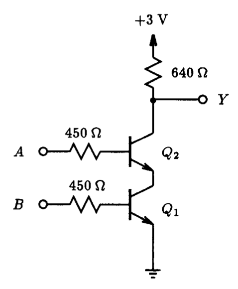
Fig. P14.2
14.2. Determine the logic function implemented by the circuit shown in Fig. P14.2 by cycling through the 4 possible inputs using Spice.

Fig. P14.3
14.3. Consider the circuit in Fig. P14.3. If VCC=5 V, R_C=R_B=1 kOhm, with the aid of Spice, determine the voltage levels at Y and Y-bar when the set and reset inputs are inactive but following an interval in which S was high while R was low? Assume that the transistors have device parameters: IS=10 fA, betaF=100, betaR=1, VA=50 V, tauF=0.1 ns, Cje=1 pF and Cjc=1.5 pF.
14.4. For the diode-transistor logic (DTL) gate shown in Fig. P14.4, use Spice to determine the logic levels: VOH, VOL, VIL and VIH. Then, calculate the corresponding noise margins. Assume that the transistor has device parameters: IS=10 fA, betaF=100, betaR=1, VA=50 V, tauF=0.1 ns, Cje=1 pF and Cjc=1.5 pF. Further, assume a base-collector shorted transistor for the pn junction diodes.
14.5. Repeat Problem 14.4 above, but for a fan-out of 5.

Fig. P14.4
14.6. For the DTL gate of Fig. P14.4, with the aid of Spice, determine the total current in each supply and also the gate power dissipation for the two cases: vY high and vY low. Then, find the average power dissipation in the DTL gate. Use the same transistor parameters given in Problem 14.4.
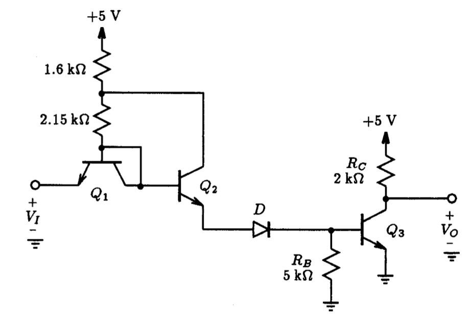
Fig. P14.7
14.7. Consider the DTL gate of Fig. P14.7 when the output is low, and the gate is driving N identical gates. Assume that the transistors have Spice parameters IS=10 fA, betaF=50, betaR=0.1, and VA=50 V. Further, assume a base-collector shorted transistor for the pn junction diodes. Use Spice to determine:
(a) the output voltage for N=0, and
(b) the maximum allowed fan-out N under the constraint that the output voltage does not exceed twice the value found in (a).
14.8. For the DTL gate of Fig. P14.7 use Spice to plot the base current supplied to Q3 when vi goes high and the reverse current that flows out of its base when vi goes low. What is the storage time ts associated with Q3. Assume that the transistors have device parameters IS=10 fA, betaF=100, betaR=1, VA=50 V, tauF=10 ns, Cje=1 pF and Cjc=1.5 pF. The diode is realized by short circuiting the base to the collector of a npn transistor.
14.9. A variant of the T2L gate shown in Fig. 14.1 is being considered in which all resistances are tripled. For both inputs high, use Spice to determine all node voltages and branch currents. Assume that the transistors have Spice parameters IS=1.81 fA, betaF=50, betaR=0.1, and VA=100 V.

Fig. P14.10
14.10. For the BJT circuit shown in Fig. P14.10, use Spice to determine the following:
(a) What logic function is performed?
(b) Determine VOL and VOH?
(c) Find VIL and VIH at the A input when both the B and C inputs are held at ground potential.
(d) What are the noise margins?
(e) Determine the average power dissipated by this gate when both input B and C are held at ground.
Assume that the transistors have device parameters IS=10 fA, betaF=100, betaR=1, VA=50 V, tauF=0.1 ns, Cje=1 pF and Cjc=1.5 pF. Further, assume a base-collector shorted transistor for all pn junction diodes. For the Schottky-diodes assume: IS=1 pA, n=1, Cj0=0.2 pF, fo=0.7 V and m=0.5.
14.11. For the ECL circuit shown in Fig. P14.11, determine, with the aid of Spice, the following:
(a) Find VOH and VOL.}
(b) For the input at B sufficiently negative for Q_B to be cut off, what voltage at A causes a current of 1/2 mA to flow in QR.
(c) Repeat (b) for a current in QR of 0.99 mA.
(d) Repeat (c) for a current in QR of 0.01 mA.
(e) Use the results of (c) and (d) to specify VIL and VIH.
(f) Find NMH and NML.
Assume that the transistors have Spice parameters IS=10 fA, betaF=50, betaR=0.1, and VA=75 V.
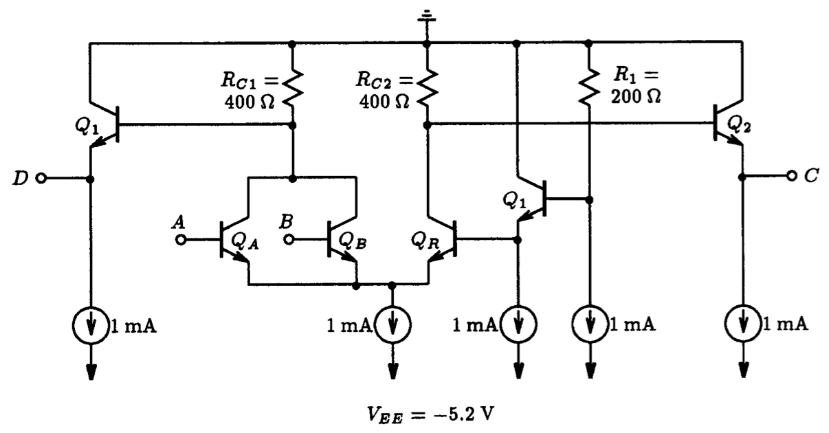
Fig. P14.11
14.12. For the BiCMOS and CMOS NAND gates shown in Fig. 14.20, with the aid of Spice, compute the propagation delay time for the following capacitive loads: 10 fF, 100 fF, 1 pF and 10 pF. The propagation delay time is defined as the time between the midway points of the input and output voltage waveforms. Sketch the delay-time versus load capacitance for both gates. What can you conclude from these results? Use the same transistor models and dimensions as was used in section 14.3.

Fig. P14.13
14.13. Shown in Fig. P14.13 is an example of a practical BiCMOS NAND gate. With the aid of Spice, compute the voltage and current waveform associated with a 1 pF load capacitor. Use the same transistor models and dimensions as was used in section 14.3.