
Fig. 3.33 A 5 V regulated power supply
* sample section from SPICE for Microelectronics Circuits, 1st Ed, by G. W. Roberts and A. S. Sedra, Saunders College Publishing, 1992.
To complete this section on rectifier circuits we shall analyze a commonly
used power supply configuration with Spice. Consider the circuit shown in
Fig. 3.33. It can be thought of as consisting of three parts: a full-wave
peak rectifier, a zener diode voltage regulator and the load. The peak rectifier
circuit acts to supply a relatively stable DC voltage to the zener regulator
which, in turn, reduces any voltage fluctuation (ripple) that appears on
it. In addition, the voltage regulator acts to maintain a constant voltage
across the load for a wide range of load currents. Resistor R_Isolation
is used for Spice simulation purposes and plays no role in the circuit function.
Fig. 3.33 A 5 V regulated power
supply
Let us consider using the circuit configuration shown in Fig. 3.33 to
design a 5 V power supply for an application that requires a maximum load
current of 20 mA. The 120 V-rms AC household voltage is stepped down to
a 12 V-peak level using a center-tapped transformer with each coil on the
secondary side having a turns ratio of 14:1 with respect to the primary
coil. Further, we have at our disposal a zener diode that has V_Z=5.1 V
at a current of 20 mA and has a dynamic resistance r_z=10 Ohms. We also
know that the minimum zener diode current must be limited to 5 mA if we
are to maintain the diode in its breakdown region. Assuming that the input
voltage to the voltage regulator circuit ranges between 9 and 12 V, we choose
the current limiting resistor R from the expression (derived in Section
3.5 of Sedra and Smith):
R = ( V_min - V_Z0 - r_z I_Zmin ) / ( I_Zmin} + I_Lmax ) (3.11).
Thus, we obtain R=160 Ohms. As a point of reference, under worst-case
conditions, the expected minimum output voltage is about 4.95 V as calculated
from the expression, V_Omin=V_Z0 + r_z I_Zmin.
The size of the smoothing capacitor is to be determined so that the voltage
applied to the regulator circuit does not go below 9 V. Assuming that the
peak voltage appearing across the secondary-side of the center-tapped transformer
is 12 V, then the worst-case ripple voltage must be limited to no more than
3 V. We shall limit the ripple voltage to a more conservative 1 V level
in case the peak voltage level changes. We can then estimate the size of
the capacitor we require by using the formula for the ripple voltage provided
in Table 3.3 for a full-wave peak rectifier. Substituting R=160 Ohms, V_r=1
V, V_P=11.2 V (accounting for a 0.8 V diode drop) and f=60 Hz, we get C=583
uF. This capacitance may seem large but is typical of the size of capacitor
used in power supplies.
A Regulated Power Supply
* zener diode subcircuit
.subckt zener_diode 1 2
* connections: | |
* anode |
* cathode
Dforward 1 2 1mA_diode
Dreverse 2 4 ideal_diode
Vz0 4 3 DC 4.9V
Rz 1 3 10
* diode model statements
.model 1mA_diode D (Is=100pA n=1.679 )
.model ideal_diode D (Is=100pA n=0.01 )
.ends zener_diode
** Main Circuit **
* ac line voltage
Vac 1 0 sin(0 169V 60Hz)
Rs 1 2 0.5
* transformer section with center-tap
Lp 2 0 10mH
Ls1 3 4 51uH
Ls2 4 5 51uH
K12 Lp Ls1 0.999
K13 Lp Ls2 0.999
K23 Ls1 Ls2 0.999
* isolation resistor
Risolation 4 0 100Meg
* full-wave peak rectifier circuit
D1 3 6 D1N4148
D2 5 6 D1N4148
C 6 4 583uF
R 6 7 160
* zener diode
XZ1 4 7 zener_diode
* load
Rload 7 4 500
* diode model statement
.model D1N4148 D (Is=0.1pA Rs=16 CJO=2p Tt=12n Bv=100 Ibv=0.1p)
** Analysis Requests **
.OPTIONS ITL5=0
.TRAN 0.5ms 200ms 0ms 0.5ms UIC
** Output Requests **
.plot TRAN V(7,4) V(6,4)
.probe
.end
Fig. 3.34 The Spice input file for calculating the time-varying output voltage of the 5 V regulated power supply shown in Fig. 3.33. Changing the ITL5 internal parameter of Spice through an .OPTIONS command resets the transient analysis total iteration limit. Setting ITL5=0 increases this limit to infinity.
To investigate whether our design meets the required specifications, we
shall simulate the power supply circuit shown in Fig. 3.33 with an initial
load resistance of 500 Ohms. This load should draw an average current of
no more than 10 mA -- well within the maximum load current condition. The
Spice deck for this circuit is seen listed in Fig. 3.34. The transformer
is represented by a primary inductance of 10 mH, and the two coils on the
secondary-side are each assigned a value of 51 uH. The two rectifier diodes
are assumed to be modeled after the commercial diode type 1N4148.
The first analysis that we shall perform with Spice is to determine whether
the output voltage is nominally 5 V. This can be determined by observing
the voltage across the load resistance. Due to the presence of the large
smoothing capacitor C, a long charge-up time will be necessary before the
power supply circuit reaches steady-state. Therefore, a request for a long
transient analysis is necessary to observe steady-state behavior. Here we
have selected that the transient be computed over a 200 ms interval. Moreover,
because of this long time interval, many iterations of the transient analysis
algorithm will be performed by Spice. If the number of iterations performed
by Spice exceeds 5000, Spice will stop the analysis. To allow more than
5000 iteration, we can reset this limit by reassigning a new value to the
Spice internal parameter ITL5. This is accomplished by including an .OPTIONS
command line in the Spice deck with the new value of ITL5, ie.
.OPTIONS ITL5=0.
Note that Spice recognizes that ITL5=0 really means ITL5=infinity, or
in other words, ignore this test and allow as many iterations as is necessary.
In almost all cases, the number of iterations required to complete a given
analysis is not know a priori, thus it is simplest to just use ITL5=0.
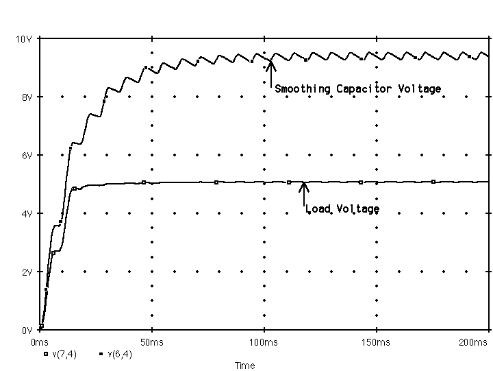
Fig. 3.35 The voltage across the smoothing capacitor C of the peak rectifier, and the output voltage across the 500 Ohms load resistance.
On completion of the Spice analysis, the voltage waveform that appears across
the 500 Ohms load resistor is shown in Fig. 3.35. Also shown is the voltage
that appears across the smoothing capacitor C. As we can see, the voltage
across the capacitor has an average value of about 9.5 V and a peak-to-peak
ripple of 0.25 V. In contrast, the voltage across the load resistor is quite
close to 5 V. Using the cursor facility of Probe, we find that the load
voltage ripples slightly, between 5.065 and 5.080 V, a ripple voltage of
only 15 mV. We therefore see that the above power-supply design is operating
quite close to the nominal design, providing an output voltage of 5 V at
a load current of about 10 mA.
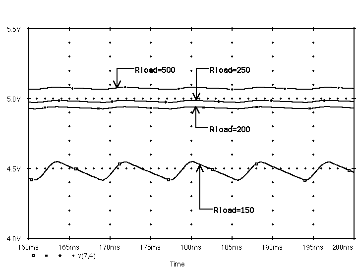
Fig. 3.36 The output voltage waveform from the 5 V power supply for load resistances of 150, 200, 250 and 500 Ohms. The voltage regulation is lost at a load resistance of 150 Ohms.
To see the effect of larger current demands on the power supply, consider
reducing the load resistance. In order to compare the effect of different
loads, we shall re-simulate the circuit with load resistances of: 150, 200
and 250 Ohms. Assuming that these load resistances do not significantly
affect the output voltage, they would correspond to a load current of: 33.3
mA, 25 mA and 20 mA, respectively. Using the same Spice deck as shown in
Fig. 3.34 with only the value of the load resistance altered, we concatenated
three similar files, together with the original one having a load of 500
Ohms, into one file for processing. As a result of the analysis, we display
a view of the output voltage over the time interval 160 to 200 ms. As is
clearly evident, for load resistances greater than and including 200 Ohms,
the output voltage is maintained very near the 5 V level with very little
ripple visible. However, for a load resistance of 150 Ohms, we see that
the output voltage level has dropped down to an average value of about 4.5
V. Also, we see that the ripple voltage associated with this signal has
increased significantly. This suggests that the output voltage is no longer
being regulated. This is because the zener diode has been starved of its
current and has turned off.
We conclude that the power supply circuit shown in Fig. 3.33 will provide
a constant 5 V output level for load currents at least as large as 25 mA.